![]()
![]()
4.3
Receiver Operation
Fig.7
shows the UART’s (CDP6402R) operation and explains its’ job that is to
transfer the Serial Data into Parallel Data, which is then available on the
Receiver Buffer Register Pins, RBR 8 to 1. When the UART receives a byte, it
signals this by asserting the Data Received (DR) line high. This will stay high,
until the Data Received line is reset. This is done by making Data Received
Reset (nDRR) low, thus the use of the Inverter. The LCD Display also requires a
high to low Transition on it's enable pin to accept data.
Data is received in serial form at the RRl input. When no data is being received, RRI input must remain high. The data is clocked through the RRC. The clock rate is 16 times the data rate. Receiver timing is shown in Figure 7.
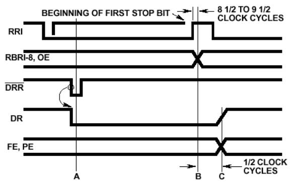
Fig.
7 Receiver
timing diagram
(A)
A low level on DRR clears the DR line. (B) During the first stop bit data is
transferred from the receiver register to the RB Register. If the word is less
than 8 bits, the unused most significant
bits will be a logic low. The output character is right justified to the least
significant bit RBR1. A logic high on OE
indicates overruns. An overrun occurs when DR has not been cleared before the
present character was transferred to the RBR. (C) 1/2 clock cycle later DR is
set to a logic high and FE is evaluated. A logic high on FE indicates an invalid
stop bit was received. A logic high on PE indicates a parity error.